


What is high speed PCB design
Contents
- What is high speed PCB design?
- High speed PCB design rules and challenges
- Trace length tuning
- Impedance
- Track shape
- Termination
- Grounding
- Components location
- Placement of ground polygons on the layers close to the signal layers
- Crosstalk
- Tips for high speed PCB design based on the first-hand experience
- CAD Software Helpful Features
- Final Thoughts
Nowadays, a printed circuit board of any modern electronic device should meet the requirements of technologically advanced solutions. That is why high speed PCB design has become a hot topic for hardware engineering professionals.
All high-tech devices are designed with a high speed PCB thanks to which the size of the devices is getting smaller, data transfer is getting faster and the devices themselves are becoming more functional and handy.
That is why it is really important for every PCB designer to know high speed board design basics. If you are in the loop already, go ahead, take a shot and design a high speed PCB. Doing this, you will get the necessary skills and experience, uplevel yourself, and stay a go-to engineer.
Our team has already had such experience performing on high speed PCB design projects. So we decided to write this article to underscore the relevance of its topic and share our personal experience.
We hope our high speed design guidelines supported by first-hand recommendations will be helpful to designers who make their first steps in exploring this area.
What is high speed PCB design?
First of all, let us clarify what high speed PCB design is. To make it simple, check a list of characteristic features below. If you can tick at least one of them, you know what we are talking about in this article.
- High speed interfaces such as HDMI, Ethernet, SATA, PCI Express, USB, Thunderbolt, etc. are used for the fast data transfer.
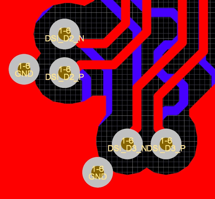
- The circuit consists of several sub-circuits connected to each other through high speed interfaces (LVDS, DSI, CSI, SDIO, DDR3, etc.).
- Signal propagation time over the track is at least ⅓ of the signal rise time.
- The digital signal frequency is of 50MHz and over.
- The size of the printed circuit board is very small and the location of the components becomes a real challenge (especially when you come across a high speed interface layout).
To sum up, high speed PCB design is applied to devices with PCBs working at high frequencies with the use of high speed interfaces. With that, the amount of data and speed of its transfer mean the world.
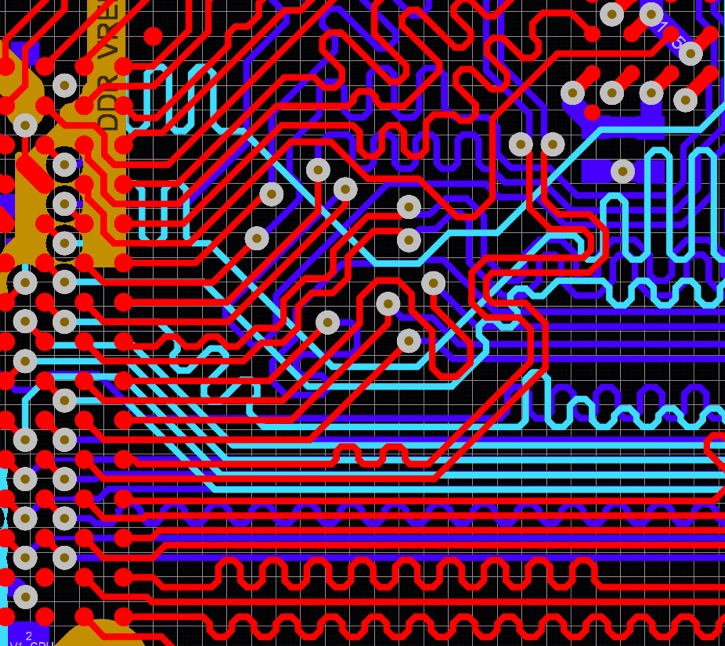
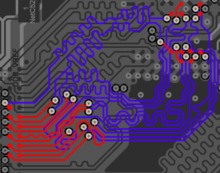
This picture illustrates a part of high speed PCB design developed by our engineers for a home automation system. Our team managed to meet all the challenges and achieved great results in the development of a tablet-style smart home head unit.
High speed PCB design rules and challenges
As in every engineering process, there are certain rules and directions on how to design a high speed PCB. Let us consider the key points and challenges which may arise at the same time.
Trace length tuning
When you use a high speed interface, you need to tune the length of the traces to synchronize signal propagation through data lines. If it is not synchronized, the interface could fail at the maximum frequency or will not work at all.
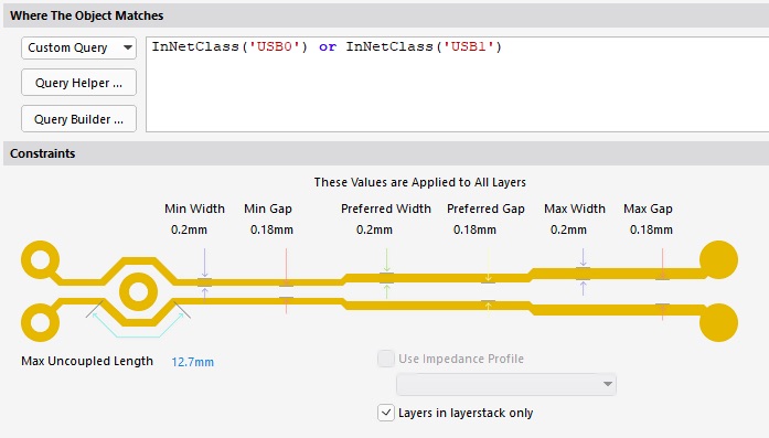
The higher the interface frequency, the higher the requirements of the length matching. As you know, there are two types of interfaces in PCB design and length tuning will be different for each of them. For a parallel interface, we tune only the lengths of the traces. The main challenge is that there are many traces with a lack of space for length tuning. For a serial interface, we unite signals into several differential pairs.
Length matching rules for differential pairs are more complicated. All traces should have the same length with a tolerance of X mm. With that, the length of the traces should be equal in each pair with a tolerance of Y mm, given that Y < X.
Aligning of the traces’ lengths leads to the loss of the distance equality between the tracks of a differential pair. You should make sure that the length of such equality-loss regions is not more than the maximum uncoupled length.
For extremely high speed interfaces, it is important to remember about the interconnecting delays inside CPUs, FPGAs, etc. Bear these delays in mind when you tune the tracks’ length.
Modern CADs have built-in tools for trace length tuning. Before you start using such tools, you should define aligning rules for each of the interfaces. It is important to know which particular rules and limitations you should define.
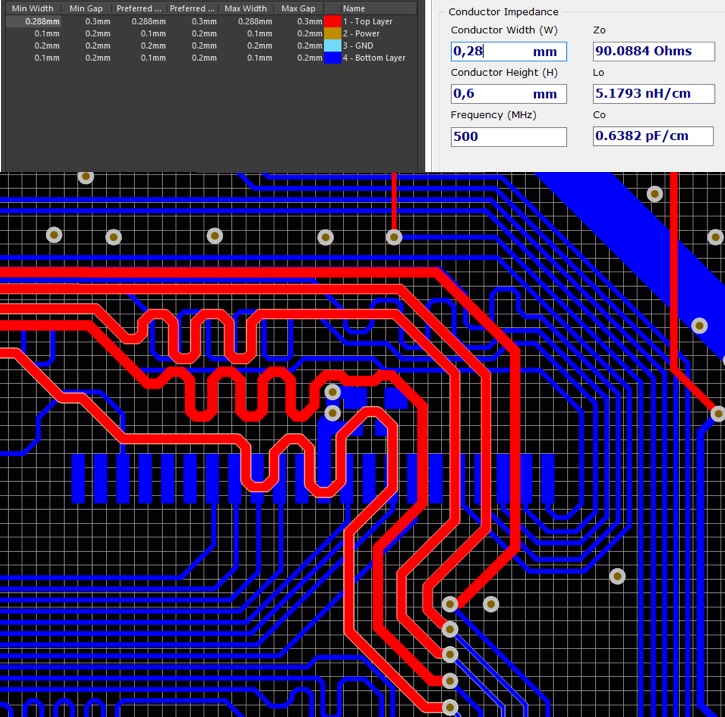
Impedance
When you make a PCB layout or a high speed PCB layout, you should observe single-ended impedance Zo as well as differential impedance Zdiff.
As a refresher: single-ended impedance is the impedance of single tracks that are not united into differential pairs. Differential impedance is the impedance between a pair of coupled tracks.
There are typical impedance values for each interface both parallel and serial.
There are also other types of impedance:
- Odd Mode Zoo (half the value of the differential impedance)
- Common Zcm (into a pair of lines with identical signals)
- Even mode Zoe (twice the common mode value)
These impedances are quite rare though you shouldn’t forget about them. The wrong single-ended or differential impedance will lead to the signal reflections inside the track. This will result in the loss of signal quality, decrease of working frequency and generation of unwanted EMI.
That is why adherence to the right impedances is one of the most important rules of the high speed PCB design.
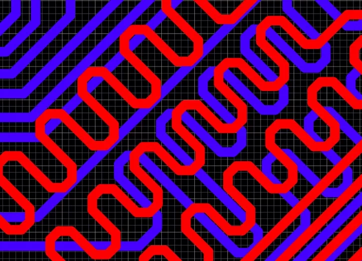
Track shape
You can hardly ever meet straight tracks from the sources to the receiver on boards. Especially in the context of high speed interfaces where you have to bend the tracks while tuning their lengths.
Ideally, tracks should have rounded, smooth corners without sharp bends. However, you need plenty of time to achieve this.
What makes such a design even more time-consuming is that you redraw each track several times during the layout optimization.
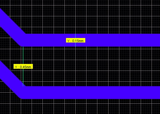
The worst case is to bend tracks at 90-degree angles. The thing is that the width of the track changes drastically at the bends. As a result, impedance changes in these places and reflections appear in the track. In the case of differential pairs, this also leads to a higher value of uncoupled length.
For this reason, the best option is to bend tracks at an angle of 45 degrees.
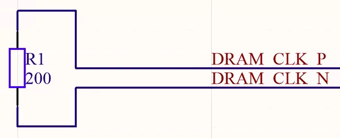
Termination
Today the most common type of termination is parallel termination. The idea is to place a resistor between the tracks of a differential pair at the end of the line, as close to the receiver as possible.
Termination makes it possible to effectively get rid of signal reflections in the tracks, therefore, upgrading the quality of data transfer. In the case of differential pairs, resistor value should be equal or a little more than Zdiff.
The low value of the resistor will cause over-termination which will adversely impact the signal quality.
Some ICs have termination resistors inside. In this case, you do not need external resistors because they will cause over-termination. That’s why it is important to learn datasheets and hardware design guides for all ICs you use.
Grounding
In most cases, you cannot trace high speed interfaces on one layer. Thus you need to move traces to the other layers with the help of vias.
GND polygons potential on different layers should be the same near signal vias. That’s why you should place GND vias as close to them as possible
Such GND vias are called stitching vias. This approach allows keeping the same GND reference all along the high speed trace.
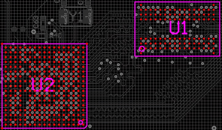
Components location
Before you start placing components connected to each other by high speed interfaces, remember that the length of the tracks is not very long. So make sure you leave enough space for the length tuning.
There is no point in placing such components very close to the interference sources, such as switching power converters.
You shouldn’t place components relating to high speed interfaces too close to the edge of the board. Such placement has a negative impact on signal quality.
The components’ location becomes a real challenge when a PCB is of a very small size. Following the location rules for high speed design, we placed the components in the most accurate manner on a small PCB for a custom IP camera.
Placement of ground polygons on the layers close to the signal layers
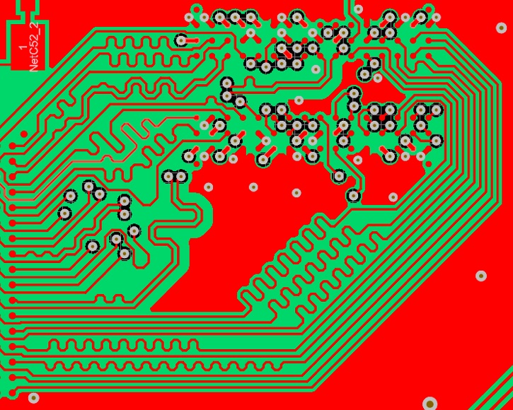
You should route tracks of high speed interfaces over a solid GND plane.
We do not recommend you route tracks over cutouts in polygons or over polygon-splits. Otherwise, you will get extra EMI, signal propagation delays, integrity violation, generation of interference and finally, degradation of the signal quality.
If the tracks happen to cross polygon-splits, it is necessary to place ceramic stitching capacitors at the place of polygons splitting. This will minimize the negative impact on the signal.
Crosstalk
Crosstalk is a phenomenon that takes place when a signal transmitted over one communication track raises an unwanted effect in the other tracks. The effect shows as a change in signal and in most cases, the tracks are neighboring.
Crosstalk depends on the length of the section where the tracks run parallel with each other. The longer the section’s length, the higher the crosstalk.
To minimize crosstalk, it is necessary to make the distance between the tracks at least three times longer than the track’s width (3W rule).
To minimize crosstalk between differential pairs, the distance between the differential pairs should be at least five times longer than the track’s width (5W rule). Keep the same distance between differential pairs and any other tracks along the full length of the differential pair.
If a differential pair serves to transmit a periodic signal, e.g. clocking, we recommend you increase the distance from this differential pair to the other differential pairs or any other tracks up to 8-10W.
Pay special attention to the tracks of asynchronous signals (enable, interrupt, reset, etc.). You should make the distance between these tracks and tracks with high speed signals as long as possible.
Sometimes we use two neighboring layers in a multilayer printed circuit board to route signals. Doing this, remember to route the tracks on one layer perpendicular to the tracks on the second layer. Thus you will avoid parallelism of the tracks and minimize crosstalk between them.
We have mentioned the basic rules of high speed PCB design but not all of them. This is a wide area of an even much wider area called PCB design.
In its turn, PCB design is a part of such a vast and multistage domain as embedded hardware development. It includes, for instance, preparation for production and selection of components. At these stages, you should consider bazillion nuances such as the device production time and the scheduled time for discontinued components, etc.
Tips for high speed PCB design based on the first-hand experience
As a team of developers who have been adept at high speed PCB design, we’ll be happy to share our experience with you. So here are some first-hand tips that you can use to streamline your workflow designing a high speed PCB.
As we pointed out in the previous section of this article, tuning of traces’ length is a crucial aspect in high speed design. The main problem is that the built-in tools of modern CADs allow controlling the overall length of the traces.
However, if the tracks of a high speed interface pass on several layers, you should align both the overall length of the traces and sections of the tracks on each layer. The reason for this is that signal propagation time is different on different layers.
To control the section lengths, it is easy to use an excel or google spreadsheet. You should add the lengths of the track sections located on different layers. Although you add data manually, this approach helps you tune the trace length with the required accuracy.
Another important aspect that we mentioned above is an impedance issue. Our strong recommendation, or even a must-do, here is to ask your manufacturer about their PCB stacks and parameters of the tracks. You need this to get the required impedance on different layers.
This is really essential because calculated values can differ from the actual impedance. Depending on each manufacturer, there is a slight difference in the characteristics of materials that affect impedance.
Before you set the design rules of high speed interfaces on your board, you should choose the right manufacturer and check all the details. Ask them about the stack-up options they have for the number of layers you need. Learn about the length of the tracks and distance between them to obtain the required single-ended and differential impedance.
To get the required impedance of some tracks on manufactured boards, you should indicate these tracks on the design.
Don’t forget to ask your manufacturer to perform the impedance control procedure. Such a procedure will add to the cost of manufacturing but will allow the designer to increase the quality of high speed signals on the PCB.
It is always very useful to get new knowledge and adopt experience from other developers for both newcomers and advanced engineers. Our engineers are no exception. They are constantly trying to replenish their store of knowledge and move with the times.
One of the most efficient methods of doing that is to take various courses and training programs.
For newcomers, this course can help teach how to start, what to do first, what to do next, how to check every part of the PCB, how to create output documentation, and a lot of other information. Experienced engineers will be able to learn a lot of useful tips and tricks which can save plenty of time.
CAD Software Helpful Features
One more helpful tool that can leverage your high speed PCB design is your CAD software. We at here able to use Cadence Allegro, Altium Designer, EAGLE, KiCad, and others. The new functionality added in Altium Designer 20 facilitates a high speed layout design to a large extent. We would like to show you some useful features that we learned first hand.
Propagation Delay is a new Altium function which is very helpful for high speed PCB design. This function allows a designer to see the length of the signal traces and the signal propagation delay at the same time.
The Propagation Delay feature can be really handy in the places where you need a certain signal delay on a specific track. You can also set a rule in the Design Rule Check (DRC) to check that the selected tracks meet the preset conditions, for example, to minimize the delay difference between differential pairs.
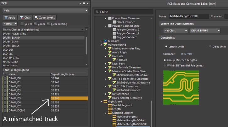
The screenshot above shows how the rule in the DRC works. We set an acceptable propagation value and after the rules are checked, a mismatched track is detected.
Another new feature proposed in Altium Designer 20 is Interactive Sliding. This function tackles a number of issues that you might face during high speed layout. The picture below shows a preferred way to lay out a BGA microcontroller.
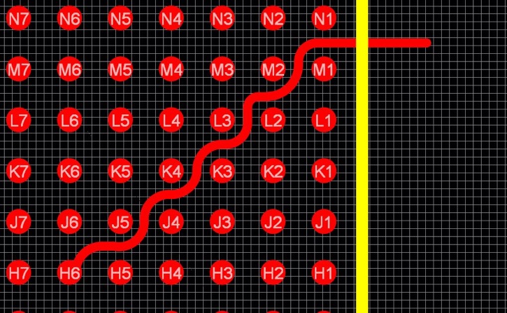
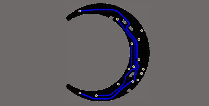
Interactive Sliding assists greatly in the design of non-standard printed circuit boards, such as ring-shaped PCBs.
Altium has a wide range of interesting features including their collaboration with GitLab and SolidWorks.
You can look through all GitLab threads, track the detailed change history, and push changes directly from Altium.
SolidWorks Collaboration makes it possible to edit a board straight in SolidWorks. You open a 3D model, place the components, save changes, and then just edit the tracks in Altium.
Final Thoughts
As you see, high speed design is a challenging but really interesting subject which leaves a lot of space for research and practice. As a PCB designer, you should definitely delve into that subject to meet the needs of the age.


0 Comments