- Home
- Training
- _Sort Term Courses
- __Basic PCB Design Course
- __Advanced PCB Design
- __High Speed PCB Design
- _Internship
- __3 Months Internship
- __6 Months Internship
- __1 Year Internship
- _Industrial Training
- __For B.Tech Students
- __For Diploma Engineering
- _Final Year Project
- __M. Tech Final Project
- __B. Tech Final Project
- __Diploma Eng Project
- Internship
- _3 Months Internship
- _6 Months Internship
- _1 Year Internship
- Mega Menu
- Documentation
- _Web Doc
- _Video Doc
- EDA Tools
- _Multi DropDown
- __DropDown 1
- __DropDown 2
- __DropDown 3
- _ShortCodes
- _SiteMap
- _Error Page
- Design Support
- _Web Doc
- _Video Doc
- Download Center

Popular Topics
Hot Technology
5/random/post-list
Labels
Marking Diode Poles on Silkscreen Layer...
Vijay Gupta
February 22, 2021
Marking Diode Poles on Silkscreen Layer
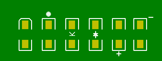
Diodes are a type of circuit component which conducts electricity typically in one direction as they have a low resistance in one direction and very high resistance in the other direction. This directionality requires that the component be assembled in a particular orientation in order to operate as intended. To ensure proper installation by your circuit assembler, it is important to include a mark on the silkscreen layer to identify which terminal is the anode and which terminal is the cathode.However, a board that has a (+) silk screen marking is not enough information to tell the assembly house how to correctly insert a diode because there are different types of diodes. For zener or barrier diodes, the (+) marking may or may not be the cathode of the component. Furthermore, an LED usually has a (+) anode, but not all the time. To verify the proper way to place a diode onto a PCB, it is best to use an “A” for anode or a “K” for cathode (C is used to label capacitors thus to avoid confusion we recommend K for cathode). You may also use a circuit symbol of a diode to show the orientation, however this requires more space on a board than a letter and may not be useful for dense board layouts. See the diagrams below for a comparison between ambiguous and clear diode markings.
By properly labelling your diodes you avoid the need to clarify your design intentions further and reduce the likelihood of diodes being placed incorrectly.

Ambiguous Diode Markings

Clearer Diode Markings
Ratings:
Platform:
WindowsYou may like these posts
Google Review
Subscribe Us
Contact form

Popular Posts
Categories
Search This Blog
PCB Design Tips

Function keys (shortcut keys) in Allegro | OrCAD PCB Editor
March 21, 2021
Controlled Impedance Routing Using Altium Designer
February 23, 2021

PCB Interview Tips and Glossary
February 22, 2021

How to create a Centroid / X-Y Data / Pick & Place File.
February 22, 2021
What is high speed PCB design
February 22, 2021
PCB Design Hot Topics
5/random/post-list
Footer Menu Widget
Created By SoraTemplates | Distributed By e aadhar card


0 Comments